

![]()
![]()
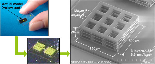
3D lattice pattern
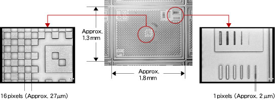
Resolution pattern
Biochip
ACCULAS® can be used to make biochips, which will play a prime role in the fields of drug discovery and regenerative medicine. The microchip arrays shown in the photo are in a plane structure, but when ACCULAS® is used, 3-D chip arrays for cell culture can be manufactured.
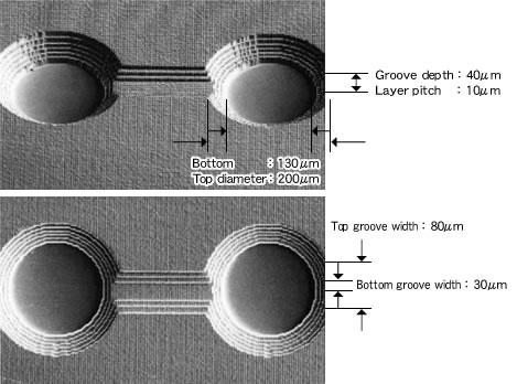
Micro Flow Channels
Micro flow channels are usually formed using a method in which a glass plate is etched, thereby creating simple channels, to which a second glass plate top is bonded. However, when ACCULAS® is used, flow channels of all shapes can be formed. Furthermore, 3D flow channels can be perfectly created without using a top.ACCULAS® brings much more freedom to the design of flow channels, allowing designs that perfectly match job requirements.
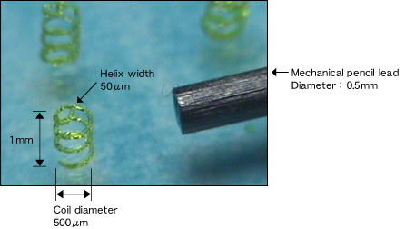
Micro Springs, Cantilevers, Probes, and MEMS (Microsystems)
The photo shows an example of micro spring production using ACCULAS®. The 0.5 mm diameter is the same diameter as the lead in a mechanical pencil. Micro springs have applications in cantilevers and micro probes. In the field of MEMS, the use of ACCULAS® will enable far more flexible designs for 3-D products, leading to new innovations in MEMS manufacturing.
Electroforming Mold Masters (Production Masters for Imprint Molds)
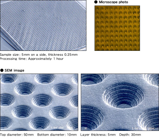
The photo on the under shows 2,500 tapered holes formed on a plate measuring only 5 mm x 5 mm. The upper diameter of each hole is 50 microns, and the lower diameter is 10 microns, with a depth of 30 microns.This construction would be extremely difficult to achieve using conventional micro processing methods. However, when ACCULAS® is used, the plate can be formed in just one hour. Using the plate as a master, Ni-electroformed molds were made and used as nanoimprint molds (for light guiding plate, diffusion plate etc. ) .
The pillar structure measures 150 microns by 50 microns and the conical structure has a lower diameter of 150 microns and is 150 microns tall were also built by ACCULAS®. After going through the Ni-electroforming and resin removal processes, the molds were used as metal molds for imprint molding of thermo-plastic resin.
Photonic Crystal and Photonic Fractal (Ceramic Micro Solids)
Photonic crystal is a complex 3-D solid that could not be made without the stereo-lithography technique. The object is in fact a ceramic. After modeling a resin containing ceramic nano powder, and following dewaxing and sintering, a ceramic solid was made.
Micro Parts
ACCULAS® makes possible the prototype production and small-lot manufacturing of super-small parts such as micro connectors and micro gears, tasks that are not achievable using conventional stereo-lithography systems.
Maskless Lithography System for Photoresists
As ACCULUS® is equipped with light sources of not only 405 nm but also 365 nm, it can be used in wider applications such as a maskless lithography system for photoresists.
![]()
| Top of ACCULAS® | ACCULAS® : Examples of Modeling | Product Inquiries |